New hybrid semiconductor material for sustainable hydrogen production
Efficient catalyst for water splitting
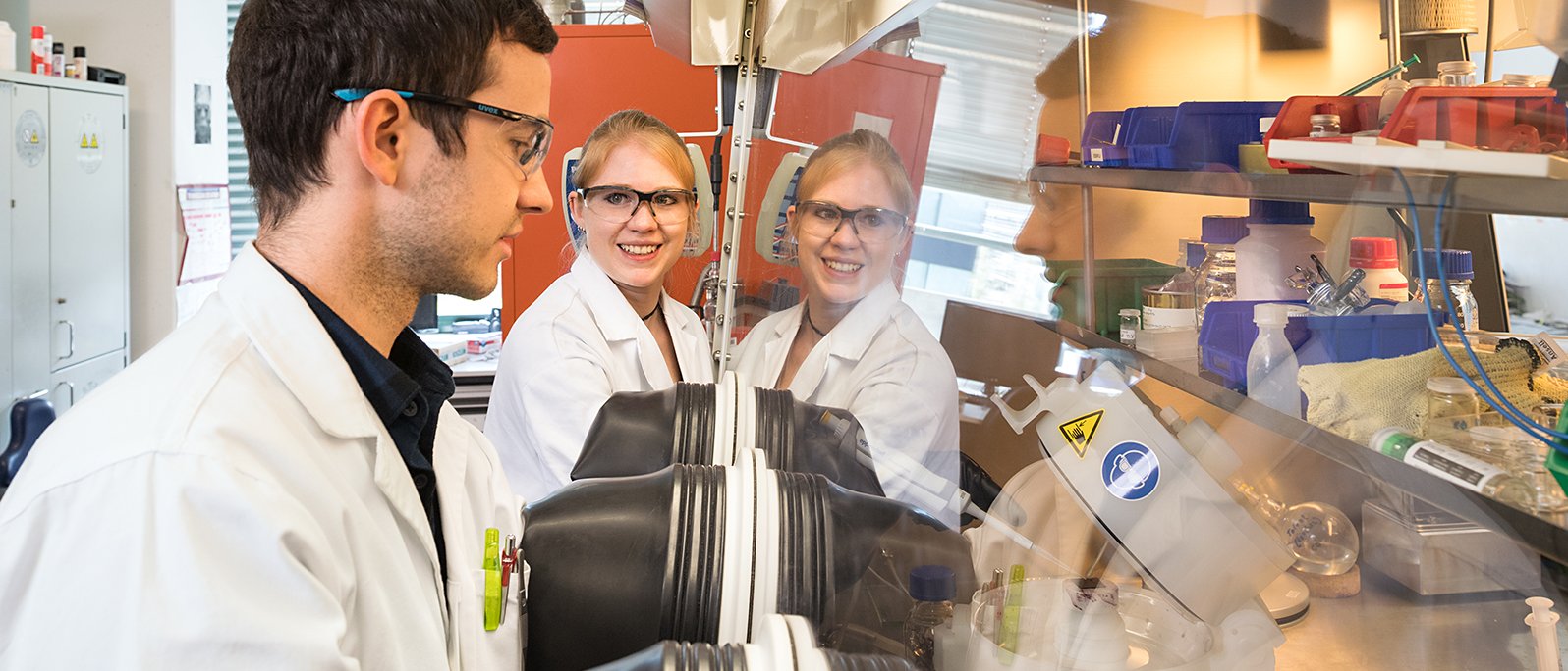
An international team led by TUM chemist Tom Nilges and engineer Karthik Shankar from the University of Alberta have now found a stable yet flexible semiconductor structure that splits water much more efficiently than was previously possible.
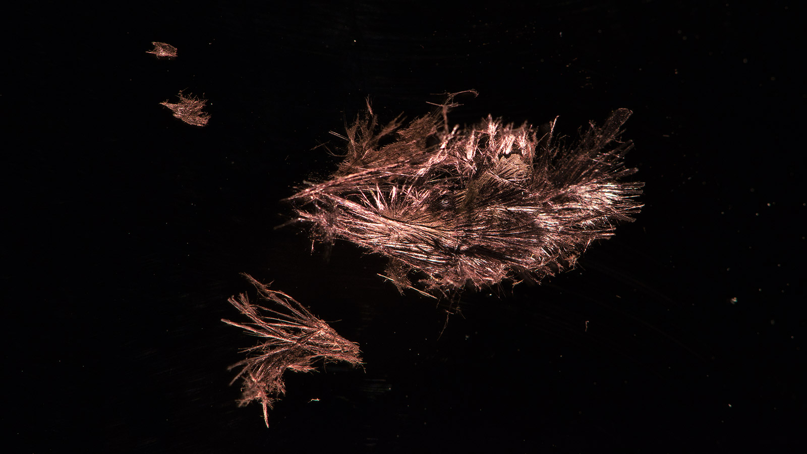
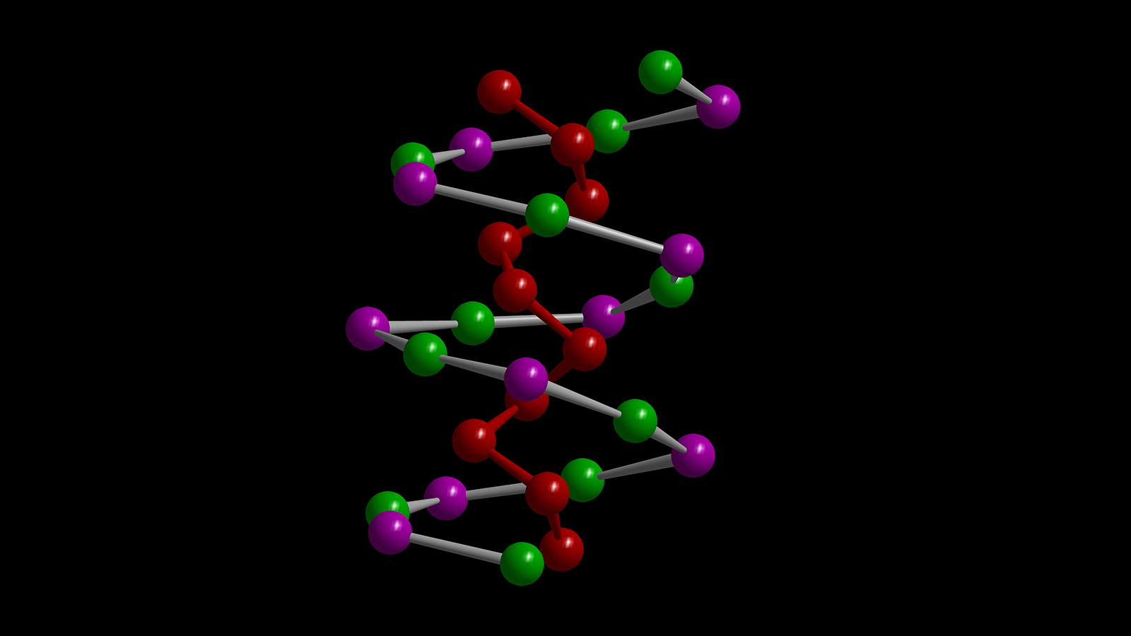
An inorganic double-helix compound comprising the elements tin, iodine and phosphorus (SnIP) forms the core of the structure. It is synthesized in a simple process at temperatures around 400 degrees Celsius. The SnIP fibers are flexible and, at the same time, robust as steel.
"The material combines the mechanical properties of a polymer with the potential of a semiconductor," says Tom Nilges, Professor of Synthesis and Characterization of Innovative Materials at the Technical University of Munich. "From this, we can manufacture flexible semiconductor components in a further technical step."
Soft shell with a hard core
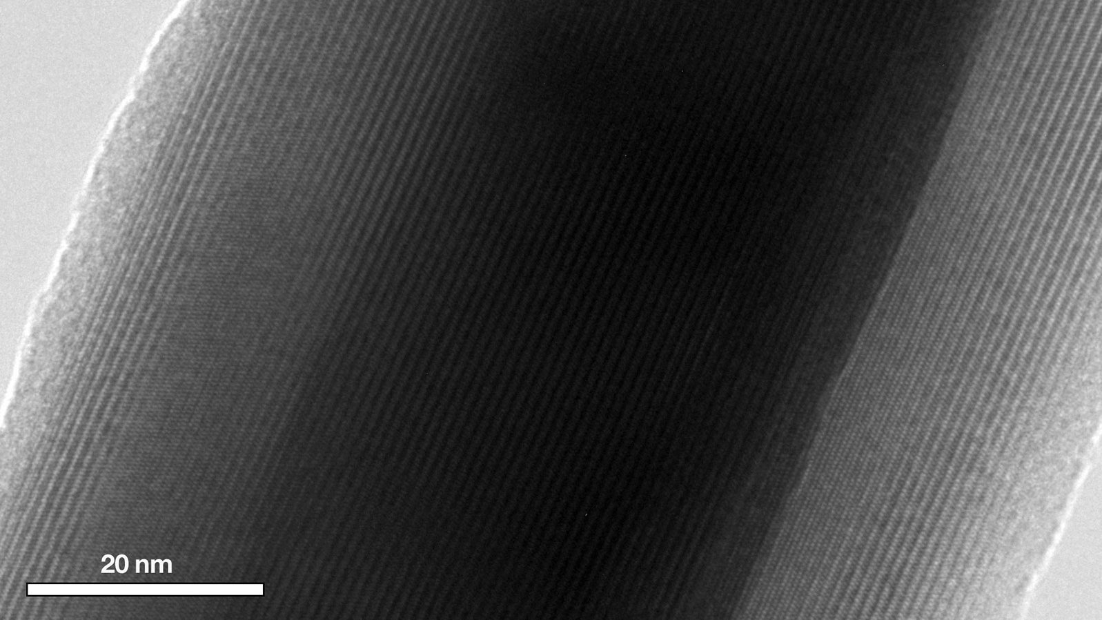
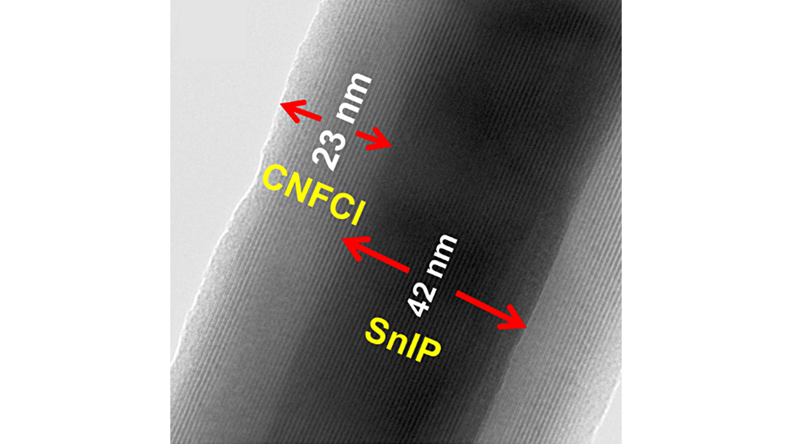
The use as a water splitting catalyst is the first application for the unusual material. The chemists prepared nanoparticles from each of the starting substances and mixed the suspensions of these two nanoparticles with each other. The result was a structure with a hard but flexible SnIP-core and a soft carbon nitride shell.
Measurements show that the resulting heterogeneous structure is not only significantly more stable than either of the initial materials. It also splits water four times more efficiently than was previously possible, making it interesting as a material for producing cheap hydrogen or to chemically store surplus electricity from wind farms.
One-dimensional fibers
Knowing that the catalyst’s great efficiency stems primarily from its large surface, the chemists increased the surface area by splitting the SnIP fibers into thinner strands. A mixture of 30 percent SnIP and 70 percent carbon nitride turned out to be the most effective.
The thinnest fibers comprise several double helix strands and are merely a few nanometers thick. The material is in principle one-dimensional. Wrapping it in carbon nitride allows the material to retain its high reactivity while becoming more durable – thereby making it more suitable as a catalyst.
Flexible semiconductors may trigger new hype
But the one-dimensional SnIP double-helices also open the door to very different kinds of applications. The researchers would be particularly keen on obtaining single strands of SnIP. These would then be right or left handed – with their own respective very special optical properties. This makes SnIP a highly attractive material for optoelectronics.
"We were able to show theoretically that many other compounds of this kind are possible. Currently we are working on the synthesis of these materials," says Nilges. "Flexible, inorganic, nanometer-sized, 1D semiconductors might create as much hype as 2D layered materials like graphene, phosphors, or molybdenum disulfide do today."
Hybrid material for watersplitting
Flexible and Ultrasoft Inorganic 1D Semiconductor and Heterostructure Systems Based on SnIP
Claudia Ott, Felix Reiter, Maximilian Baumgartner, Markus Pielmeier, Anna Vogel, Patrick Walke, Stefan Burger, Michael Ehrenreich, Gregor Kieslich, Dominik Daisenberger, Jeff Armstrong, Ujwal Kumar Thakur, Pawan Kumar, Shunda Chen, Davide Donadio, Lisa S. Walter, R. Thomas Weitz, Karthik Shankar and Tom Nilges
Advanced Functional Materials, 2019, 1900233 – DOI: 10.1002/adfm.201900233
The research was funded by the European Community as part of the Calipso project, the National Research Council of Canada (NRC), the Natural Sciences and Engineering Research Council of Canada (NSERC) and the German Research Foundation (DFG) as part of the International Graduate School ATUMS (TU Munich and University of Alberta, Canada), the Cluster of Excellence e-conversion and Nanosystems Initiative Munich (NIM), the "Solar Technologies go Hybrid" (Soltech) project of the Free State of Bavaria, the Center for Nanoscience (CeNS), Future Energy Systems (FES), CMC Microsystems, and Diamond Light Source Ltd..
Technical University of Munich
Corporate Communications Center
- Andreas Battenberg / TUM
- battenberg@zv.tum.de
- presse@tum.de
- Teamwebsite
Contacts to this article:
Prof. Dr. Tom Nilges
Professorship for Synthesis and Characterisation of innovative Materials
Technical University of Munich
Lichtenbergstr. 4, 85748 Garching, Germany
Tel.: +49 89 289 13111 – E-Mail
